Dutch Semiconductor Equipment Giant Faces Technology Delay Challenge: Hybrid Bonding Prospects and Market Game
Introduction
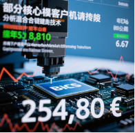
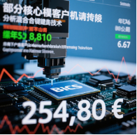
On July 15, 2026, shares of Dutch semiconductor equipment manufacturer Besi Semiconductor (Besi) experienced significant volatility, falling 6.7% in a single day to close at EUR 254.80. This market reaction stemmed from key news: some core customers of the company will delay adoption of its advanced hybrid bonding technology. Despite the short-term negative impact, Besi's stock has still accumulated over 90% gains YTD, driven by surging downstream chip demand. This event not only highlights the technology iteration risks in the semiconductor equipment industry but also reflects the delicate balance of supply and demand in the global chip supply chain. This article systematically analyzes and discusses Besi's technology advantages, the deep reasons behind customer delay decisions, the company's fundamentals, and industry prospects.
Strategic Position of Hybrid Bonding Technology and Besi's Competitive Moat
Core Driver of Advanced Packaging Technology
Hybrid bonding technology is a cutting-edge process in advanced packaging, whose core lies in direct copper-to-copper bonding to achieve high-density, low-latency interconnects between chips. As Moore's Law approaches physical limits, the cost and difficulty of traditional process scaling have risen sharply, making advanced packaging a key path to sustaining performance improvement. Particularly in fields requiring extremely high bandwidth and low power consumption, such as AI chips, high-performance computing (HPC), and 3D NAND flash, hybrid bonding is considered an indispensable underlying support.
As a world leader in semiconductor assembly equipment, Besi has built a deep technology moat in the hybrid bonding field. The company's Die-to-Wafer and Wafer-to-Wafer hybrid bonding equipment, with high-precision alignment systems, low defect rates, and high throughput, have long dominated the market. Its customers include top global chip manufacturers and packaging and testing firms, such as TSMC, Samsung, Intel, and Micron.
Technology Leadership and Market Recognition
In recent years, with the explosion of AI large model training demand, heterogeneous integration of HBM (High Bandwidth Memory) and logic chips has become mainstream. Hybrid bonding is the key process for achieving HBM stacking and processor integration. Leveraging its first-mover advantage, Besi has secured a large number of orders and revenue growth. Its 2025 financial report showed year-over-year revenue growth of over 60%, with hybrid bonding-related equipment contributing about 35% of revenue, and gross margins consistently above industry average.
Deep Analysis of Core Customer Delay Reasons
Technology Maturity and Mass Production Risk Considerations
However, any cutting-edge technology inevitably faces challenges of yield, cost, and stability during the transition from lab to mass production. Besi's core customers delaying adoption of its hybrid bonding technology may involve the following factors:
-
Yield Ramp Below Expectations: The hybrid bonding process imposes extremely strict requirements on cleanliness, temperature control, and alignment accuracy. In actual mass production, some customers may find that the current equipment's overall yield has not reached the threshold for commercial mass production (e.g., above 99.5%). For high-value chips, even a 0.1% defect rate could lead to billions of dollars in losses, so customers prefer to delay adoption and wait for further technology maturation.
-
Alternative Technology Route Competition: Although hybrid bonding is seen as the future mainstream, it is not the only option. Microbump and TSV technologies still have cost advantages in some scenarios. Some customers may choose to continue using existing technologies during the transition while waiting for upgraded versions of hybrid bonding equipment.
-
Capital Expenditure Rhythm Adjustment: The semiconductor industry has typical cyclical characteristics. Despite strong AI demand currently, downstream customers must balance macroeconomic uncertainty, interest rate environment, and geopolitical risks when making expansion decisions. Since Q2 2026, some chip manufacturers have begun tightening capital expenditure budgets, prioritizing operational efficiency of mature production lines and becoming cautious about purchasing cutting-edge technology equipment.
Besi's Short-Term Performance Pressure but Long-Term Logic Unchanged
After the announcement, Besi's stock fell immediately, reflecting market concerns about short-term order reductions. However, looking at the company's overall revenue structure, hybrid bonding equipment, while growing rapidly, is not the only revenue source. The company also has a solid customer base in traditional packaging equipment such as wire bonders and die attach machines. More importantly, the 90% stock gain YTD is based on a comprehensive explosion of downstream chip demand—whether AI chips, automotive electronics, or IoT terminals, all have sustained demand for high-performance packaging equipment. Therefore, a single customer's delay decision is more of a normal adjustment in the technology verification process rather than a signal of industry trend reversal.
Deep Drivers of >90% YTD Gain and Market Sentiment
Chip Demand Explosion: Dual Engine of AI and HPC
Looking back at the first half of 2026, the global semiconductor equipment market experienced a strong upcycle. Driven by the deployment of large models like ChatGPT and GPT-5, orders for AI chips from companies like Nvidia, AMD, and Google surged, in turn boosting shipments of upstream equipment suppliers. As a leader in packaging equipment, Besi directly benefited from this wave. Additionally, the electrification and intelligence trends in automobiles boosted demand for power semiconductors and sensors, further expanding the equipment market.
Financial Data and Order Visibility
Besi's Q1 2026 financial report showed revenue up 82% year-over-year, net profit growth exceeding 100%, and order backlog hitting a record high of approximately EUR 1.5 billion. Management emphasized in the earnings call that the customer concentration of the product portfolio is declining, with emerging customers from China, Europe, and North America accounting for a significantly higher share. This diversified customer structure effectively spreads the risk of demand fluctuations from a single customer.
Short-Term Market Sentiment Volatility and Long-Term Resilience
The 6.7% stock decline, from a technical perspective, was a panic sell-off triggered by negative news, but it did not break key support levels. Investors should focus on whether the decline is accompanied by fundamental deterioration. According to company announcements, the delay only involves some core customers, and these customers explicitly stated they will continue to cooperate with Besi for technology iteration, with no signs of customer loss. Meanwhile, other customers (such as a Korean memory giant) have even accelerated their adoption of hybrid bonding technology. Therefore, the short-term correction instead provides an entry opportunity for long-term investors.
Industry Landscape and Competitive Outlook
Future Evolution of Hybrid Bonding Technology
Despite the delay, hybrid bonding remains firmly positioned as the core technology for advanced packaging over the next decade. As 3D IC and chiplet architectures become industry consensus, the demand for higher bonding density, smaller pitch, and lower thermal resistance will continue to drive technological progress. Besi is already developing next-generation hybrid bonding equipment, aiming to reduce bonding pitch from the current 40 μm to below 10 μm and achieve wafer-level fully automated docking.
Competitor Dynamics and Besi's Advantage Retention
Currently, Besi holds about 60% of the global hybrid bonding equipment market. Main competitors include Japan's Tokyo Electron (TEL) and Austria's EV Group. TEL has accumulated certain technology in wafer-level bonding, while EV Group excels in temporary bonding and debonding equipment. However, Besi remains far ahead in Die-to-Wafer bonding accuracy and production speed. In addition, the company leverages the Netherlands' optical and precision machinery industrial cluster to establish a supply chain advantage that is difficult to replicate.
Conclusion
Overall, the stock decline of Besi is a short-term sentiment shock triggered by core customers delaying adoption of its hybrid bonding technology and does not change the company's long-term value growth logic. Fundamentally, the >90% YTD gain is supported by solid performance, and the two trends of chip demand explosion and increasing advanced packaging penetration will continue to drive growth. Technically, the maturation of hybrid bonding takes time; customer delay is a normal part of the technology verification process and may even promote more robust industry standard setting. Looking ahead, Besi is expected to maintain its leading position in the semiconductor equipment sector through technology leadership, customer diversification, and supply chain resilience. For institutional and individual investors focusing on long-term semiconductor investment, this may be a critical moment to evaluate entry opportunities.
This article represents an industry analysis perspective only and does not constitute investment advice. Market risks exist; invest with caution.