Hybrid Bonding Technology Ushers in New Era of Chip Stacking – Besi Semiconductor's Path to Industry Leadership
Keywords: Hybrid Bonding; Thermo-Compression Bonding; Besi Semiconductor; Chip Interconnect; Advanced Packaging
Introduction
As Moore's Law approaches physical limits, the semiconductor industry is undergoing a paradigm shift from "scaling" to "integration." Advanced packaging technology, especially three-dimensional stacking solutions, has become a key path to sustaining performance improvement. Among many interconnect technologies, hybrid bonding, with its ability to achieve precise fusion at the molecular level, is moving from laboratories to mass production and is considered the core process for next-generation high-density memory and logic chip integration. In this cutting-edge track, Besi Semiconductor, with years of technology accumulation and mass production experience, has firmly established its industry leadership. Its technology roadmap and market layout are profoundly influencing the evolution of global advanced packaging.
I. Hybrid Bonding: Precision "Suturing" at the Molecular Level
Traditional chip stacking mostly uses thermo-compression bonding (TCB), which melts solder to connect upper and lower chips through heating and pressing. However, as storage capacity demand surges, the limitations of TCB in process precision and space efficiency become increasingly prominent. In contrast, hybrid bonding technology achieves a qualitative leap: it uses chemical mechanical polishing (CMP) to create ultra-flat surfaces, pre-bonds through van der Waals forces between dielectric layers at room temperature or low temperature, and then causes copper contacts to diffuse through annealing, ultimately achieving chip-to-chip bonding at the molecular level.
The core advantages of this technology lie in two aspects. First, extremely low bonding pitch: hybrid bonding can reduce the gap between chip layers to sub-micrometer levels, typically just tens of nanometers, far below the solder layer thickness of several micrometers in TCB. Second, higher interconnect density: by not relying on solder balls or bumps, hybrid bonding can arrange tens of thousands of copper contacts per unit area, thus supporting larger bandwidth data transmission. Together, these two points create hybrid bonding's unique value in 3D stacking: integrating larger capacity storage in limited space while reducing power consumption and latency.
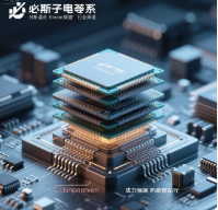
Figure note: In the hybrid bonding process, the dielectric layers of the upper and lower chips are pre-bonded first, then copper contacts are interconnected during annealing, forming a compact stacked structure.
II. Besi Semiconductor: From Pioneer to Frontrunner
In this high-barrier track of hybrid bonding, Besi Semiconductor is not only a technology pioneer but also one of the few companies currently achieving large-scale mass production. Its success stems from strategic deployment at three levels.
First, the ultimate pursuit of process precision. Hybrid bonding has far higher requirements for surface roughness, cleanliness, and particle control than traditional processes. Besi has independently developed proprietary CMP and wet cleaning processes that achieve surface roughness below 0.5 nm at the wafer level and ensure nanoscale consistency in copper pad recess depth. This "molecular level" process control is key to ensuring bonding yield and reliability.
Second, systematic integration of equipment and materials. Unlike general manufacturers that rely on external equipment procurement, Besi has deeply customized bonding equipment in terms of design, temperature control system, and alignment accuracy, forming a closed-loop capability from material handling to bonding completion. This vertical integration model not only reduces mass production costs but also enables rapid iteration of process parameters to meet customers' growing customized demands for storage density.
Third, continuous deep cultivation of the customer ecosystem. Currently, Besi has established cooperation with major global memory chip manufacturers and logic chip giants. Its hybrid bonding solutions are widely used in products such as high-bandwidth memory (HBM), 3D NAND, and CIS image sensors. Especially in the HBM field, with the explosive demand for memory bandwidth driven by AI computing chips, hybrid bonding has almost become the standard interconnect technology for HBM3 and future HBM4, and Besi holds about 30% market share in this space, making it an undisputed leader.
III. Comparison with Thermo-Compression Bonding: Why Hybrid Bonding is the Future?
To better understand the technical advantages of hybrid bonding, let's compare it with the still widely used thermo-compression bonding in detail.
| Dimension | Thermo-Compression Bonding (TCB) | Hybrid Bonding |
|---|---|---|
| Bonding medium | Solder (tin, indium, etc.) or conductive adhesive | Copper-copper direct bonding + dielectric layer |
| Bonding temperature | 250-350°C | Room temperature pre-bonding + annealing below 200°C |
| Interlayer gap | Several micrometers | Tens of nanometers |
| Interconnect pitch | 40 μm or more | <10 μm (extendable to 1 μm) |
| Current carrying capacity | Limited by solder electromigration | Copper interconnect, higher reliability |
| I/O density per unit area | Low | 2-3 orders of magnitude higher |
| Thermal stress | Large, prone to warpage | Small, low-temperature process more friendly |
From the table, it can be seen that while TCB still has advantages in maturity and cost, when facing the stacking demands of HBM memory with 12, 16, or even more layers, its limited interconnect density and larger thermal stress have become bottlenecks. In contrast, hybrid bonding, with its ultra-small pitch and low-temperature characteristics, can not only integrate more memory layers within the same package size but also effectively reduce chip warpage and improve system reliability.
Of course, hybrid bonding is not without challenges. Its equipment cost is high, the requirements for wafer flatness and cleanliness are almost stringent, and the production ramp-up speed is slow. However, as leading companies like Besi continuously optimize processes, the unit bonding cost of hybrid bonding is decreasing at approximately 15% per year, and it is expected to achieve cost crossover with TCB in most high-end applications by 2027.
IV. Market Prospects and Industry Transformation
According to the latest report from Yole Group, the hybrid bonding market is expected to grow from approximately USD 500 million in 2024 to over USD 5 billion by 2030, with a compound annual growth rate of 45%. This growth is mainly driven by three major drivers:
- AI and High-Performance Computing: Large model training and reasoning require massive bandwidth, and the number of layers in HBM and similar memory architectures continues to increase, creating rigid demand for hybrid bonding.
- 3D NAND Flash: As layer counts exceed 600, traditional through-hole technology faces scaling limits; hybrid bonding can replace part of the through-hole connections to achieve better cell density.
- Heterogeneous Integration Trend: Integrating logic, memory, analog, and other functional chips into a single package via hybrid bonding helps break fab node limits and achieve "system-level performance" improvements.
In this wave, Besi Semiconductor faces both opportunities and challenges. On one hand, its first-mover advantage and technology barriers will allow it to benefit long-term in the high-end market; on the other hand, giants like TSMC, Samsung, and Intel are also increasing R&D investment in hybrid bonding, trying to catch up through capital and ecosystem power. The future evolution of industry patterns depends not only on process precision and cost control but also on who can achieve mass production adoption in key customers' next-generation products first.
Conclusion
Hybrid bonding technology is reshaping the boundaries of chip stacking with unprecedented precision. It extends Moore's Law in the "vertical dimension," providing a feasible engineering path for leaps in storage density and data transmission bandwidth. As the industry leader in this track, Besi Semiconductor has built significant competitive barriers through deep process accumulation, vertical integration capabilities, and a broad customer ecosystem. However, rapid technology iteration and strong entry by giants also mean the leading position needs constant consolidation.
For the semiconductor industry, hybrid bonding is not just a process option but represents a new design philosophy—no longer pursuing extreme scaling of a single chip, but achieving overall system performance breakthroughs through clever three-dimensional interconnects. In this sense, Besi's exploration may be a microcosm of the technology evolution in the next decade: craftsmanship between molecules, vastness in stacking.