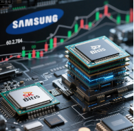
Memory Chip Giants' Technology Dilemma: Hybrid Bonding Questioned, Where Do Samsung and SK Hynix Go?
Keywords: Hybrid Bonding; 3D Stacking; Samsung Electronics; SK Hynix; Advanced Packaging; Memory Chip
Introduction
As the global semiconductor industry accelerates into the "post-Moore era," advanced packaging technology has elevated from a supporting process to a core competitiveness. Among them, hybrid bonding technology, with its extremely high interconnect density and excellent electrical performance, is regarded as a key path to break through traditional scaling bottlenecks and achieve three-dimensional (3D) stacked memory chips. However, according to reports from Korean tech media ZDNet citing anonymous industry insiders, two memory chip giants—Samsung Electronics and SK Hynix—are questioning whether to introduce hybrid bonding technology into their top-tier chip stacking products. This dynamic not only reflects deep disagreements in technology routes but could also impact the future development landscape of high-bandwidth memory (HBM) and 3D NAND flash. This article will delve into the logic behind this decision and its potential impact from dimensions such as technical principles, industrial background, customer considerations, and market reactions.
Overview of Hybrid Bonding Technology: From Concept to Competitive Focus
Hybrid bonding, also known as direct copper bonding, is an advanced packaging process that achieves vertical interconnect between chips through simultaneous metal-to-metal and dielectric-to-dielectric bonding. Compared to traditional micro-bump (μbump) or through-silicon via (TSV) technology, hybrid bonding can achieve sub-10 micron pitch, significantly reducing parasitic capacitance and resistance, and improving signal transmission speed and energy efficiency. This characteristic makes it ideal for HBM3E, HBM4, and future high-capacity 3D NAND stacking.
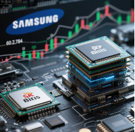
The figure above visually shows the layered structure of hybrid bonding: the copper pads of the upper and lower chips are directly fused under thermocompression, while the surrounding dielectric layer (e.g., SiO₂) also achieves seamless connection. This process eliminates the underfill step required in traditional bonding, thus supporting thinner chips and shorter signal paths. However, its manufacturing difficulty is extremely high, with almost stringent requirements on surface flatness, cleanliness, and alignment accuracy; any nanoscale defect can lead to bonding failure. Therefore, despite significant theoretical performance advantages, mass production yield and cost control remain unresolved challenges.
Deep Reasons for Customer Questions: Technology Maturity, Cost, and Path Dependency
1. Technology Maturity and Yield Bottleneck
According to insiders, Samsung Electronics and SK Hynix's hesitation about hybrid bonding technology stems first from its low maturity. Although academia and some equipment suppliers (e.g., Applied Materials, Tokyo Electron) have demonstrated lab-level results, transferring hybrid bonding from experimental lines to mass production still faces numerous difficulties. For example, micro-contaminants or particles on the chip surface can easily cause voids at the bonding interface, leading to thermomechanical stress concentration and early failure. For Samsung and SK Hynix, their existing HBM products (e.g., HBM3E) already use mature processes based on TSV and micro-bumps, with stable yields above 85%, while current hybrid bonding yields may be below 70%, implying higher unit costs and capacity loss.
2. Uncertainty of Return on Investment
Hybrid bonding requires new wafer bonding equipment, cleaning equipment, and precision inspection tools, with a complete production line investment easily exceeding billions of dollars. Against the backdrop of volatile memory chip prices and incomplete recovery of downstream demand, the two giants must carefully assess the marginal benefits of technology upgrades. For DRAM and NAND, whether performance improvements can translate into product premiums remains questionable. For example, while HBM4 requires higher bandwidth and lower power consumption, customers (e.g., Nvidia, AMD) are more concerned about system-level cost and supply stability than purely pursuing interconnect density limits. Samsung and SK Hynix naturally do not want to sacrifice short-term profits for "technology supremacy."
3. Path Dependency and Differences in Technology Reserves
Notably, the two companies' attitudes toward hybrid bonding are not entirely consistent. Samsung Electronics, leveraging its advantages in system semiconductors and logic foundry (e.g., 3nm GAA process), has accumulated earlier experience in hybrid bonding. Its subsidiary Samsung Semiconductor Institute (SSI) has developed a hybrid bonding solution for 3D DRAM and plans trial production in 2026. In contrast, SK Hynix relies more on its existing HBM technology advantage—the company holds over 50% market share in HBM3E, and its "TC-NCF" (Thermal Compression Non-Conductive Film) process is more mature in mass production. Therefore, SK Hynix has stronger incentives to maintain the existing route and avoid shaking market position due to technology iteration. The stock performance mentioned in the ZDNet report (Samsung up 2.75%, SK Hynix down 3.38%) to some extent reflects the market's interpretation of the two companies' strategic differences: if Samsung adopts hybrid bonding first, it may gain long-term competitive advantage; if SK Hynix lags, it may face the risk of declining product competitiveness.
The Dilemma of Technology Evolution: A Fork in the Road for the Memory Industry
1. Game in the HBM Field
In the high-bandwidth memory field, the JEDEC standard has defined wider interfaces and higher speeds for HBM4 but does not mandate hybrid bonding. Current mainstream solutions still increase stacking layers (from 12 to 16) and optimize TSV. The advantage of hybrid bonding mainly lies in reducing the thickness per layer (thinning DRAM dies to below 20 μm), allowing more layers within the same package height. However, adopting hybrid bonding requires simultaneous adjustments in DRAM die manufacturing processes (e.g., using "die-to-wafer" bonding instead of "wafer-to-wafer"), which is a transformative change for highly standardized HBM production lines. Samsung and SK Hynix must balance performance gains against supply chain risks.
2. Potential Transformation in 3D NAND
Beyond DRAM, hybrid bonding's application in 3D NAND is also drawing attention. Currently, NAND Flash relies mainly on charge trap cells and higher layer counts (e.g., 238 layers, 300 layers) to increase storage density, but increasing layers worsens word line resistance and RC delay. Hybrid bonding can be used to fabricate CMOS peripheral circuits separately from the memory array and then stack them via hybrid bonding, thereby optimizing wafer area utilization. This "separated" architecture (e.g., Kioxia/Western Digital's CUA process) has shown potential. However, Samsung, as the NAND leader, has independently developed its V-NAND technology route; whether to introduce hybrid bonding to counter competition from Micron and SK Hynix still requires rigorous cost-benefit analysis.
Market Reaction and Future Prospects: Wait or Accelerate?
1. Cautious Attitude in the Short Term
Based on current information, Samsung Electronics and SK Hynix have not explicitly abandoned hybrid bonding but are in a state of "questioning" and "evaluation." This cautious attitude aligns with the semiconductor industry's consistent logic of "mature technology first." Especially considering that memory chip market demand may recover in 2026 but capacity utilization is still ramping up, companies prefer to allocate capital expenditures to expanding mature process capacity rather than risk investing in unproven cutting-edge technology. Industry analysts expect that large-scale application of hybrid bonding in HBM may be postponed to 2027 or later in the second half of 2026.
2. Long-Term Trend Irreversible
However, from the historical pattern of technology evolution, the potential of hybrid bonding will eventually be released. As scaling reaches physical limits, 3D stacking will become the only path to continuously improve chip integration. Logic chip giants like TSMC and Intel have already applied hybrid bonding in 3D SoIC and plan mass production by 2025. Although the memory sector moves slower, market demand will force technological progress. For example, future AI training tasks require HBM bandwidth exceeding 2 TB/s; relying solely on increasing I/O count will cause chip area expansion, making hybrid bonding's high-density interconnect a necessity.
3. Game Between Suppliers and Ecosystem
The questioning by Samsung and SK Hynix also serves as a stress test for the supply chain maturity. Equipment manufacturers need to demonstrate 0.1 μm-level alignment accuracy and throughput of tens of thousands of wafers per hour; materials suppliers need to provide flatter wafer surface treatment solutions; and test equipment makers need to develop high-speed, high-precision bonding interface inspection systems. If these links fail to achieve breakthroughs in 2026, the two major customers may further delay adoption. Conversely, if equipment yields improve to acceptable levels and cost decline curves accelerate, 2027 could become the "commercial year" for hybrid bonding.
Conclusion
Samsung and SK Hynix's questioning of hybrid bonding technology is not simply technological conservatism but a deep weighing of technology risk based on business rationality. In the current volatile memory chip market with changing competitive landscape, any major process change could reshape a company's fate. Hybrid bonding undoubtedly represents the direction of advanced packaging, but its commercialization path still requires time, capital, and ecosystem synergy. For the industry, this technology review triggered by customer questioning is precisely a necessary process to push the entire ecosystem toward maturity. Over the next two years, we may see Samsung and SK Hynix find their own balance between "incremental improvement" and "leapfrog innovation," and the ultimate fate of hybrid bonding technology will be jointly determined by yield, cost, and actual downstream application demand.
(Approximately 2,460 words)